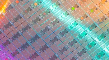
Putting 50 billion transistors into a microchip the size of a fingernail is a feat that requires manufacturing methods of nanometer-level precision—layering of thin films, then etching, depositing, or using photolithography to create the patterns of semiconductor, insulator, metal, and other materials that make up the tiny working devices within the chip.
The process relies heavily on solvents that carry and deposit materials in each layer—solvents that can be difficult to handle and toxic to the environment.
Now researchers led by Fiorenzo Omenetto, Frank C. Doble Professor of Engineering at Tufts, have developed a nanomanufacturing approach that uses water as the primary solvent, making it more environmentally compatible and opening the door to the development of devices that combine inorganic and biological materials. The research is reported in the journal Nature Nanotechnology.
The challenge in using water as a solvent is that the materials it comes into contact with during manufacturing are often hydrophobic, meaning they repel water. Similar to the way water beads on a well-waxed car, the surface of a silicon wafer or other material may resist being coated evenly with a water-based material.
Omenetto and his team at the Tufts University Silklab discovered that the protein building block of common silk, called silk fibroin, can significantly enhance water’s ability to evenly cover virtually any surface, depending on how much fibroin is added.
Other such surfactants that change the property of water are used in commercial production to solve this problem, but silk fibroin can be used in significantly smaller quantities, yields superior quality results, and is biologically and environmentally friendly.
“This opens up a huge opportunity in device fabrication,” said Omenetto. “Not only can one deposit water-soluble materials and metals on silicon, but on all sorts of polymers. We can even deposit and print biological molecules on virtually any surface with nanometer precision.”
Omenetto and his team had demonstrated this ability in earlier studies creating a hybrid silicon-biological transistor that can respond to the environment, transition between digital and analog processing, and could even be a precursor to neuromorphic (brain-like) devices.
Biological molecules have been used in combination with electronics to detect glucose in blood, antibodies indicating infection, and DNA fragments to identify mutations, for example, but integrating them into common nanomanufactured devices like microchips could allow the design of the next generation of biosensors and processors that respond to health and environment.
The nanodevices demonstrated in the current study using water-based processing include many components that are in widespread use today in computers, smartphones, solar cells and other technologies:
- Indium gallium zinc oxide transistors used primarily in display technologies, flexible electronics, image detection and touch screens
- Aluminum oxide insulators used in transistors to control the flow of electrons
- Nickel oxide films used in optical filters, solar cells and transparent displays, and
- Perovskite films used in high efficiency solar cells, light emitting diodes, light detectors, lasers and memory storage
The performance of these components matched that of their commercially developed counterparts. In fact, water-based manufacturing of microchips and other nanodevices can be easily substituted into the current manufacturing process, the researchers said.
